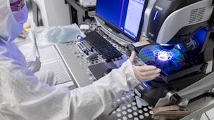
This course will cover various aspects of microelectronics and nanoelectronics. This field aims to advance and improve the functionality of electronic devices by scaling transistors to smaller feature sizes. The course will introduce you to essential concepts such as length scales, transistor actions, and feature sizes of integrated circuits. The course will also look at historical observations and trends using Moore’s Law, which currently guides and predict development of the Semiconductor industry. Most importantly, our goal is to highlight why packaging is so important and relevant today. Furthermore, we will also explore the anatomy and function of a semiconductor package, starting with substrate-level package interconnection to the motherboard. We will also describe features as we differentiate various types of packages and how they differ in materials, design, and reliability.

Introduction to Semiconductor Packaging

Introduction to Semiconductor Packaging
This course is part of Semiconductor Packaging Specialization

Instructor: Terry Alford
7,125 already enrolled
Included with
154 reviews
What you'll learn
Introduction to essential concepts such as length scales, transistor actions and feature sizes of integrated circuits.
Historical observations and trends using Moores Law
Explore the anatomy and function of semiconductor packaging.
Recognize various types of packages and how they differ in materials, design and reliability.
Skills you'll gain
Details to know

Add to your LinkedIn profile
8 assignments
See how employees at top companies are mastering in-demand skills

Build your subject-matter expertise
- Learn new concepts from industry experts
- Gain a foundational understanding of a subject or tool
- Develop job-relevant skills with hands-on projects
- Earn a shareable career certificate

There are 9 modules in this course
Welcome to Introduction to Semiconductor Packaging. In this course, Dr. Terry Alford and Dr. Mitul Modi will share various aspects of microelectronics and nanoelectronics. This field aims to advance and improve the functionality of electronic devices by scaling transistors to smaller feature sizes. Our aim is to introduce you to essential concepts such as length scales, transistor actions, and feature sizes of integrated circuits. We also look at historical observations and trends using Moore’s Law, which currently guides and predict development of the Semiconductor industry. Most importantly, our goal is to highlight why packaging is so important and relevant today. Furthermore, we will also explore the anatomy and function of a semiconductor package, starting with substrate-level package interconnection to the motherboard. We will also describe features as we differentiate various types of packages and how they differ in materials, design, and reliability.
What's included
1 video2 readings
In this module, ASU Professor Terry Alford and Intel's Dr. Mitul Modi discuss nanoelectronics, a field that aims to advance and improve the functionality of electronic devices by scaling transistors to smaller feature sizes. Professor Alford and Dr. Mitul Modi will lead you through length scales, transistor actions, the great transistor, feature sizes, integrated circuits, Moore’s Law, and new markets. You will also learn about the new challenges for semiconductor packing that arise from nanoscale fabrication.
What's included
1 video3 readings1 assignment2 plugins
In this module, Dr. Mitul Modi discusses the challenges and opportunities in semiconductor packaging. He will explain why we package semiconductor die, describe the silicon to semiconductor package process flow, and how packaging is evolving to meet new market demands. He will also introduce the concept of heterogeneous integration, which enables higher functionality by combining different types of devices in a single package. You will learn how semiconductor packaging connects the silicon circuitry to the rest of the system, manages the power and signals, protects the silicon circuitry, enables cooling of the circuitry, and enables spanning many length scales.
What's included
1 video2 readings1 assignment
In this module, you will learn about Semiconductor Packaging; the past, present, and future. Dr. Mitul Modi will explain the significance of Moore's Law, lead you through a condensed history of semiconductor packaging, and help you to identify the importance of packaging in the future, as well as why heterogeneous integration is important to the semiconductor industry.
What's included
1 video2 readings1 assignment
In this module, Dr. Mitul Modi discusses the components and types of semiconductor packages. He will explain how the IC chip and the package substrate are connected by the flip chip interconnect (FLI) and how the package is connected to the motherboard by the second level interconnect (SLI). He will also describe other features that are added to some packages depending on the design, performance, and usage requirements. Finally, he will compare different types of packages and how they differ in materials, design, and reliability.
What's included
1 video2 readings1 assignment
In this module, you will learn the structure and function of the package substrate in semiconductor packaging. Dr. Mitul Modi will describe the important features in the package substrate and discuss how the package substrate is designed for cost and performance trade-offs.
What's included
1 video2 readings1 assignment
In this module, Dr. Mitul Modi discusses the mechanical, thermal, and electrical functions of semiconductor packaging. He will talk about how the package is used to manage environmental stresses, IC heat, power, and signals and will show how packaging involves different engineering skills and knowledge.
What's included
1 video2 readings1 assignment
In this module, Dr. Mitul Modi discusses the reliability and customer ease of use. He will explain how the customer use of a package and the market use conditions affect the reliability needs and the materials/design choices for the package. You will also learn the importance of a common package footprint and second level interconnect (SLI) for motherboard design.
What's included
1 video2 readings1 assignment
In conclusion of Introduction to Semiconductor Packaging, we would like to summarize the main takeaways. We started by sharing various aspects of nanoelectronics, transistor action, reliability, and customer ease of use. Then, we explored how Moore’s Law and market use conditions affect the packages' reliability needs and the materials/design choices. At the end, we saw how the common footprint of a motherboard or socket determines a package's substrate level interconnect. Thank you for joining us.
What's included
1 video1 assignment
Earn a career certificate
Add this credential to your LinkedIn profile, resume, or CV. Share it on social media and in your performance review.
Instructor

Offered by
Explore more from Electrical Engineering

Arizona State University

Arizona State University
Why people choose Coursera for their career

Felipe M.

Jennifer J.

Larry W.

Chaitanya A.
Learner reviews
- 5 stars
77.27%
- 4 stars
17.53%
- 3 stars
3.24%
- 2 stars
0.64%
- 1 star
1.29%
Showing 3 of 154
Reviewed on Feb 20, 2024
Awesome course by Terry Alford sir,And thanks for approving my financial aid request,
Reviewed on Jun 24, 2024
very informative with simple understandable language. course content prepared is with fragmented detail... easy to understand and grasp.
Reviewed on Jul 1, 2024
It is easy to understand how important semiconductor packaging is

Open new doors with Coursera Plus
Unlimited access to 10,000+ world-class courses, hands-on projects, and job-ready certificate programs - all included in your subscription
Advance your career with an online degree
Earn a degree from world-class universities - 100% online
Join over 3,400 global companies that choose Coursera for Business
Upskill your employees to excel in the digital economy
Frequently asked questions
To access the course materials, assignments and to earn a Certificate, you will need to purchase the Certificate experience when you enroll in a course. You can try a Free Trial instead, or apply for Financial Aid. The course may offer 'Full Course, No Certificate' instead. This option lets you see all course materials, submit required assessments, and get a final grade. This also means that you will not be able to purchase a Certificate experience.
When you enroll in the course, you get access to all of the courses in the Specialization, and you earn a certificate when you complete the work. Your electronic Certificate will be added to your Accomplishments page - from there, you can print your Certificate or add it to your LinkedIn profile.
Yes. In select learning programs, you can apply for financial aid or a scholarship if you can’t afford the enrollment fee. If fin aid or scholarship is available for your learning program selection, you’ll find a link to apply on the description page.
More questions
Financial aid available,

